Types and design standards of pads in PCB design
Oct 16, 2021

2. Round pad
5. Oval pad
Two Special pads


3. Teardrop pad
Design standards for pads in PCB design


In PCB design, pad is a very important concept, PCB engineers must be familiar with it. However, although familiar, many engineers have a little knowledge of pads.
Let’s learn about the types of pads and the design standards of pads in PCB design today. The land, the basic unit of surface mount assembly, is used to form the land pattern of the circuit board, that is, a variety of land combinations designed for special component types.
The pad is used for electrical connection, device fixing, or part of the conductive pattern that combines both.
Types of PCB pads
One, common pad
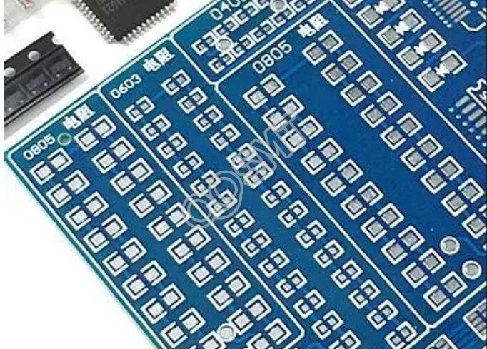
1. Square pad
It is often used when the components on the printed circuit board are large and few, and the printed wires are simple. It is easy to use this kind of pads when making a PCB by hand.
2. Round pad
It is widely used in single and double-sided printed boards with regularly arranged components. If the density of the board allows, the pad can be larger so that it will not fall off during soldering.
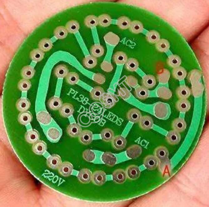
3. Island pad
The connection between the pad and the pad is integrated. It is often used in vertical irregular arrangement installation.
4. Polygonal pad
Used to distinguish pads with close outer diameters but different apertures, which is convenient for processing and assembly.
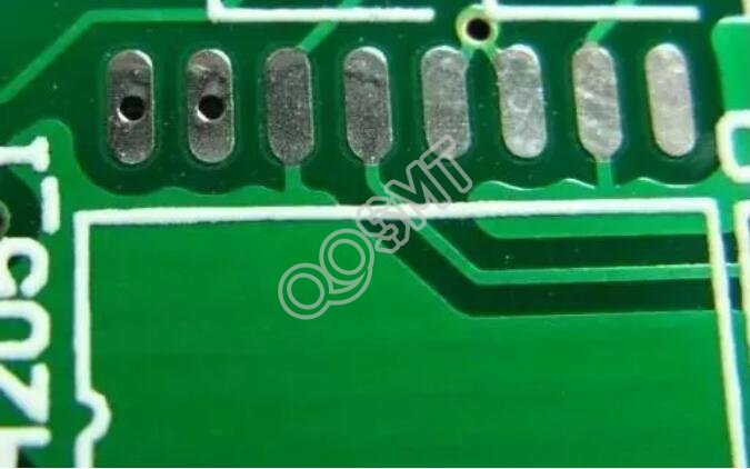
5. Oval pad
This kind of pad has enough area to enhance the anti-stripping ability, and is often used in dual in-line devices.
6. Open-shaped pad
In order to ensure that after wave soldering, it is often used when the manually repaired land hole is not sealed by solder.
Two Special pads
1. Plum blossom pad
Torx pads are usually used in large vias to ground. There are several reasons for this design:
1) The fixing hole needs to be metallized and connected to GND. If the fixing hole is fully metallized, it is easy to block the hole during reflow soldering.
2) The use of internal metal screw holes may cause the grounding to be in a poor state due to installation or multiple disassembly and assembly. However, the use of quincunx pads can ensure a good grounding regardless of the changes in the stress.
2. Cross flower pad
Cross flower pads are also called thermal pads, hot air pads, and so on. Its function is to reduce the heat dissipation of the pad during soldering, so as to prevent false soldering or PCB peeling caused by excessive heat dissipation.
1) When your pad is ground. The cross pattern can reduce the area of the ground wire, slow down the heat dissipation speed, and facilitate welding.
2) When your PCB requires machine placement, and it is a reflow soldering machine, the cross-pattern pad can prevent the PCB from peeling (because more heat is needed to melt the solder paste).
3. Teardrop pad
It is often used when the traces connected to the pads are thin to prevent the pads from peeling and the traces are disconnected from the pads. Such pads are commonly used in high-frequency circuits.
Design standards for pads in PCB design
One. The shape and size design standard of PCB pad
1. The minimum single side of all pads is not less than 0.25mm, and the maximum diameter of the entire pad is not more than 3 times the component aperture.
2. Try to ensure that the distance between the edges of the two pads is greater than 0.4mm.
3. In the case of dense wiring, it is recommended to use oval and oblong connecting plates. The diameter or minimum width of the single-sided board pad is 1.6mm; the weak-current circuit pad of the double-sided board only needs to add 0.5mm to the hole diameter. Too large the pad will easily cause unnecessary continuous soldering. The diameter of the hole exceeds 1.2mm or the diameter of the pad. The pads over 3.0mm should be designed as diamond or quincunx pads.
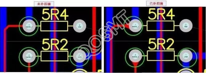
4. For plug-in components, in order to avoid the phenomenon of copper foil breaking during welding, and the single-sided connecting plate should be completely covered with copper foil; the minimum requirement for double-sided panels should be filled with teardrops.
5. All machine insert parts need to be designed as drip pads along the bent leg direction to ensure full solder joints at the bent leg.
6. The pads on the large-area copper skin should be chrysanthemum-shaped pads, which should not be soldered. If there is a large area of ground and power lines on the PCB (with an area of more than 500 square millimeters), the window should be partially opened or designed to fill the grid.
As shown in the figure:
Two. PCB pad via size standard
The inner hole of the pad is generally not less than 0.6mm, because the hole smaller than 0.6mm is not easy to process when punching the die. Usually, the diameter of the metal pin plus 0.2mm is used as the inner hole diameter of the pad, such as the diameter of the metal pin of the resistor When it is 0.5mm, the diameter of the inner hole of the pad corresponds to 0.7mm, and the diameter of the pad depends on the diameter of the inner hole.
Three, the reliability design points of PCB pads
1. Symmetry. To ensure the balance of the surface tension of the molten solder, the pads at both ends must be symmetrical.
2. Pad spacing. Too large or too small pad spacing will cause soldering defects. Therefore, ensure that the spacing between component ends or pins and pads is appropriate.
3. The remaining size of the pad. The remaining size of the component end or pin and the pad after the overlap must ensure that the solder joint can form a meniscus.
4. The width of the pad should be basically the same as the width of the component tip or pin.
Fourth, PCB manufacturing process requirements for pads
1. Test points should be added if the two ends of the chip components are not connected to the plug-in components. The diameter of the test points is equal to or greater than 1.8mm to facilitate the online tester test.
2. If the IC foot pads with dense pin spacing are not connected to the hand plug-in pads, test pads need to be added. For chip ICs, the test points cannot be placed in the chip IC silk screen. The diameter of the test point is equal to or greater than 1.8mm to facilitate online tester testing.
3. If the distance between the pads is less than 0.4mm, white oil must be applied to reduce continuous soldering when the wave crest is exceeded.
4. The two ends and ends of the SMD component should be designed with lead-tin. The lead-tin width is recommended to use 0.5mm wire, and the length is generally 2 or 3mm.
5. If there are hand-soldering components on the single panel, the tin bath should be removed, the direction is opposite to the tin passing direction, and the width of the viewing hole is 0.3MM to 1.0MM.
6. The spacing and size of the conductive rubber keys should be consistent with the actual conductive rubber keys. The PCB board connected to this should be designed as a gold finger, and the corresponding gold plating thickness should be specified.
7. The size and spacing of the pad should be basically the same as the size of the patch component.