Sub-board technology in the field of SMT electronic processing
Oct 17, 2021
The appearance and trend of electronic products, the volume of products is becoming smaller and smaller, the function is becoming more and more diversified, the components are becoming more and more sophisticated, the stability of the product is high, and the miniaturization of electronic products requires the double-sided multilayer and high interlayer of the printed board. Density interconnection greatly increases the number of components per unit area of the board, and makes the margin of the board edge smaller. High-density assembly and miniature solder joints, various product shapes, complex and diverse panels and plates, put forward higher requirements for the design and splitting process of multiple printed panels. The change of assembly board from simple segmentation to high-precision segmentation has made the reliability of board splitting face many challenges. The stress hazard and control during board splitting have also attracted increasing attention from the industry; and the correct board design and splitting process can be effective Reduce or avoid related hazards and potential failure problems.
There are many kinds of board splitting equipment, which can meet the requirements of high-density assembly board splitting process; for example, the handheld portable product assembly board has a compact shape and compact components, and there are fewer equipment that can meet its high-precision and low-stress splitting. When evaluating the splitting equipment and process for new products, it is necessary to choose the correct choice based on the product characteristics: the simple substrate of conventional linear V-slot or stamp hole jigsaw can be manually assisted by manual&Jig Split or Break; it is more difficult For cutting straight V-groove panels, you can choose Moving Cutter Separate or Air Pressure Shear; for high-density assembly panels with complex panels, curved appearance and broken tab connections , It is recommended to use CNC milling cutter-type split board (RASEM); for rigid boards, soft boards and rigid-flex board with a substrate thickness of less than 0.8mm, you can choose die punching, ultraviolet laser cutting ( UV Laser Depaneling) method of splitting. UV Laser segmentation technology, used for thin or soft board similar products, has greater advantages than traditional mechanical splitting methods. This process has high precision and no mechanical stress. For example, it is used for high-precision camera module assembly boards. The splitting effect is good. , Each splitting method has a certain scope of application in production, and the technicians should choose the correct splitting equipment and process according to the characteristics of the assembly method, the thickness and precision of the substrate, and the material.
The stress of PCBA in different ways:
The inner circuits, solder joints, and components of high-density assembly boards are usually very fragile and sensitive to various shock waves and stress damage during the manufacturing process. Therefore, the management, control and detection of the stress of the sub-board become indispensable. In the process of mechanical cutting and splitting, the shock crack and strain crack may cause potential failure of the product. When cutting the high-precision new product for the first time, the stress of the splitting board should be measured for the purpose of grasping The hazards that the cutting board may bring to the product.
Generally, the circuit board segmentation is placed in the final process of the surface assembly process, even after the ICT test and the main inspection station, so the "internal damage" caused by the splitting process is usually difficult to find. Defects such as circuit cracks in the inner layer of the assembly board, device or solder joint cracks may only be discovered when the user terminal is used, which will undoubtedly reduce the reliability of the product and the user's trust and satisfaction. To this end, eliminate poor panel interconnection design, implement design for manufacturability (DFM) without compromise, and combine the correct splitting process and stress detection control to eliminate the problem in its infancy, thereby reducing the incidence of failure .
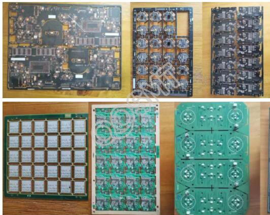
1 Board requirements and panel design of high-density assembled boards
Since the early 1990s, high-density interconnection (HDI) multi-layer printed circuit boards (Mulitlayer Printed Circuit Board) have gradually become a new generation of electronic products with the trend of multi-function and miniaturization of electronic products. Mainstream. The fifth-generation electronic assembly technology is the MPT (Micoelectronics Packaging Technology), which is becoming more and more mature, especially in handheld portable products; while the extremely small 0201 and 01005 passive components, the micro-pitch technology MPT (Microelectronics Packaging Technology) Pitch Technology's ultra-narrow pitch UFPT (Ultra Fine Pitch) devices have become popular. The sudden increase in circuit board assembly density and integration, as well as the strict environmental protection requirements of electronic products, have not only become more stringent for substrate material requirements, but also put forward the design for panel design and the Design for Fabrication of the PCB (Design for Fabrication of the PCB) Due to higher requirements, the thermal performance, flexibility and hardness of the board have been greatly increased compared to usual, so to a large extent the boarding process has increased the difficulty.
PCB manufacturability design and surface assembly are of particular interest. Design defects will inevitably bring troubles to the production process, such as increasing process difficulty, reducing production yield and efficiency, and increasing material loss. From the perspective of technology integration management, the panel design and splitting process must be carried out in the DFM (Design for Manufacture) evaluation stage. DFM mainly studies the relationship between the design of the product itself and the various parts of the manufacturing system, and uses it in product design to integrate the entire manufacturing system for overall optimization; it can reduce the development cycle and cost of the product and make it smooth Put into production, the quality is guaranteed.
1.1 Material requirements for high-density assembly boards
The gaps and distances between the surface components of the high-density assembly board and the copper foil of the inner circuit, from the edge of the board or the connection bridge (Tabs) of the board, become smaller with the miniaturization of the product.
The substrate materials of printed circuit boards are diverse. For example, common organic materials include phenolic resin paper substrates, composite substrates and epoxy glass cloth substrates, while inorganic materials include metal substrates and ceramic substrates. From the morphological point of view, PCB can be divided into rigid PCB, Flexible PCB and Rigid-Flex PCB; the complexity of the substrate material makes the splitting process cannot be simply one-size-fits-all , But must be tailored and targeted. For example, the early paper-based copper-clad laminate or the paper core composite material CEM (Composite Epoxy Material) substrate is loose, fragile and fragile. This type of substrate jigsaw uses the conventional V-Cut slot and stamp hole method through simple manual fixtures. Or electric knife cutting is easy. However, this kind of substrate has poor thermal performance and mechanical strength, so it is not suitable for lead-free or high-end products of high-density assembly boards, otherwise it is easy to cause copper skin blistering and substrate warping and other undesirable phenomena.
High-density assembly boards usually use high-quality substrates such as glass cloth epoxy resin substrate, glass fiber BT/Epoxy resin substrate and PI polyimide. The glass cloth substrate is divided into glass cloth-epoxy copper clad laminate (FR4) and Heat-resistant glass cloth-epoxy copper clad laminates (FR5), which are cost-effective and excellent in thermal performance and mechanical strength, have been widely used in lead-free and halogen-free products. The composite substrate CEM-3 is sandwiched with glass non-woven fabric, and the upper and lower surfaces are covered with glass cloth + epoxy resin; it is improved from FR-4 and has a great price advantage, and it replaces most of the glass fiber cloth with glass non-woven fabric . Their hardness and flexibility are both good, and they are currently the mainstream substrates for high-density assembly of rigid assembly boards, but the division stress of such substrates is usually relatively large. Flexible copper clad laminates (FPC) are divided into polyester resin copper clad laminates and polyimide copper clad laminates. This type of substrate has good flexibility. Special material substrates, such as metal substrates, ceramic substrates, and heat-resistant thermoplastic substrates, have complex and diverse interconnection processes, and the splitting process needs to be carefully considered in order to obtain a good splitting effect.
1.2 Jigsaw and interconnection methods for high-density assembly
There are three types of traditional circuit board interconnection, namely, the broken sign type, the stamp plate type, and the double-sided engraved V-groove. These methods may sometimes be applied comprehensively on the same assembly board. In order to facilitate breaking or cutting with pliers, the early broken-mark jigsaw has strict requirements on the size of the broken-mark (the length is not greater than 2.54 mm in width, and the width is not greater than 2 mm). The interconnection method of the stamp board is evolved on the basis of the broken label. In order to facilitate the separation of the board to reduce the strength and stress of the separation board, 5-10 small holes with a diameter of 0.8 mm are drilled in the length direction of the broken label. The board connecting bridge is named after the way the stamp board is divided. This method is used for high-density assembly boards (communication, automotive electronics, aerospace, medical equipment, precision modules, etc.) due to its low sub-board stress and guaranteed quality. The double-face engraved V-groove interconnection method is mostly used for rectangular or square regular-shaped assembly boards. This method is used when the components do not protrude from the edge of the board or the device that protrudes from the edge of the board is not the V-groove interconnection edge.
The break-off method has evolved into a bridge-joint-board interconnection method and has become the main method of high-density assembly boards. The split-board process has also been upgraded from the previous breaking method to automatic Router curve cutting, Punch punching or UV Laser Advanced technology such as segmentation. The double-sided engraved V-groove interconnection splicing method is not only the most mainstream and the most widely used in general assembly boards, but also it is still mainly used in high-density assembly boards with a substrate thickness of 1.2 mm or more.
1.3 Key Points of Jigsaw Design and Bad Interconnection
The panel design of the assembly board needs to be considered comprehensively. First of all, the shape and size of the panel are convenient for processing and the strength is sufficient. There will be no board breakage during the manufacturing process and no obvious deformation after reflow. The assembly board is easy to cut and separate. Secondly, it is necessary to consider the maximum utilization of substrate materials in order to reduce material loss and ensure circuit board assembly efficiency and product quality. Secondly, for the layout of components, pay attention to the effects of different component arrangement directions to avoid component damage due to splitting stress; usually the place closest to the interconnection of the board and the connection bridge of the board is relatively stressful, so the weak small welds when the board is assembled Point components should try to avoid these locations. At the same time, when the circuit boards of irregularly shaped single boards are assembled into connected boards, if the V-slot board is used, the board should be designed to be rectangular as much as possible (see Figure 13); the outer frame (clamping edge) of the board is recommended to adopt a closed-loop design. Ensure that the PCB panel is not easy to warp and deform after being fixed on the fixture; the board length and width are not special requirements, and should not be greater than 300*240 mm. The process clamping edge of the panel is generally 5-10 mm; for high-density assembly For thin board or FPC, the size of the jigsaw can be appropriately smaller.
In the design of the puzzle interconnection, double-numbered puzzle is adopted, that is, the front and back of the board are divided into half—commonly known as the yin and yang board. This way of paneling can save costs, such as templates, programming time, pre-production preparation and production line change time, etc., thereby greatly improving production efficiency. The yin-yang board has both a TOP surface and a BOTTOM surface on the same side of a jigsaw. After one side is produced in the production process, the other side can be turned over without changing the production process and procedures. For the Yin and Yang board, it must be double-sided mounting and does not require wave soldering and pin-in-hole reflow (Pin In Hole Reflow) processes; the TOP and BOT surfaces use the same process; the MARK point of the process edge must be symmetrical on both sides to facilitate the same procedure. Printing, placement and automatic equipment online inspection. Generally speaking, the interconnection method of the yin-yang board is different from the front and the back, and the splitting process is similar.
The following problems must be avoided when designing the interconnection of the stamp board: For the design of the stamp board, the deformation and internal stress of the substrate when the board is broken can easily lead to damage to the internal circuit, components or solder joints of the PCB, so the stamp hole interconnection There should be no traces or precision fine-pitch devices nearby. For the connection method of broken-tab connecting bridge splicing plates, CNC milling cutter-type splitting is required between the connecting plates, and the spacing of the splicing plates cannot be less than the diameter of the milling cutter. If the minimum milling cutter diameter is 1.0 mm, the minimum punching size must be greater than 1.0 mm. The protruding edge of the component covers the tab or V groove of the panel connection, which interferes with the normal operation of the panel. For the V-groove splicing board interconnection method, there should be no large devices or protruding devices near the connection points between the outer frame of the splicing board and the inner small board, and the small board and the small board. The edge of the components and the PCB board should be left The distance is greater than 1.0 mm to ensure the normal operation of the cutting tool.
2 Comparison of the separation of high-density assembly boards and common separation processes
Board splitting is sometimes called cutting board, which is to remove the unused process edges on the PCB side or separate the small boards of the multi-panel board. Although it is very simple to say, it is a very important part of the PCB assembly process. At present, there are many kinds of equipment and processes for splitting assembled boards. I will briefly explain them below and focus on the splitting equipment and processes for high-density assembly boards.
Common board splitting equipment or devices mainly include manual and clamp folding, electric or hand-push knife cutting, guillotine pneumatic cutting, CNC milling cutter type dividing machine, steel mold punching and cutting, laser cutting, and so on. Among them, electric or hand-push knife cutting and guillotine pneumatic cutting are usually mainly used for dividing the interconnection board of the V-Cut slot. These two methods are relatively widely used in current production; and high-density assembly Thicker hard boards and irregular jigsaw interconnects are mainly cut by CNC milling cutters; thin plates, soft boards, or rigid and flexible jointed boards and irregular jigsaw boards are punched with steel die, or used Ultraviolet laser cutting is more suitable. Ultraviolet laser cutting is a new type of technology that does not generate mechanical stress during the cutting process. It is used for high-density assembly of thin plates, soft plates or rigid-flex board, which has advantages compared with traditional mechanical splitting.
2.1 Milling cutter type dividing machine (Router)
Mainly used for rigid substrate segmentation. This splitting method has less cutting stress and less vibration and impact. When splitting the board, the assembly board remains fixed. The milling cutter head can move up and down or horizontally to feed, and the tool path is set according to the program. conduct. Router cutting machine is usually composed of computer intelligent control system, X, Y and Z axis AC servo motor drive system, image recognition system, high-speed positioning system and assembly board clamping device (double or single tray), and cutting dust absorption device. constitute. The router cutting program is simple to make, and the split trajectory path is set quickly, and it can easily handle circuit boards with complex shapes and different sizes. The current router cutting machine, in order to improve efficiency, usually double workbenches with two jigs, when one picks and places the board, the other can perform cutting operations, the front of the router cutting machine and the operating conditions.
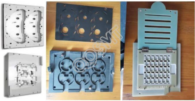
The automatic track splitter requires well-made special fixtures, which are made of aluminum alloy, anti-static bakelite or engineering plastics. The clamp is divided into two parts: the base and the gland. The magnet block (magnet diameter 5-10 mm thick 3-6 mm) needs to be embedded in the corresponding positions of the base and the four sides of the gland. The function of the magnet is to fix the base and the gland. Two positioning posts (5-12 mm in diameter) need to be installed at the diagonal corners of the fixture base, and a well-matched positioning hole is required on the gland, refer to Figure 22B. The assembly board has components where the fixture base and gland must be hollowed out, The space position and the components must have enough margins, and the components must not be touched when the fixture is pressed; in order to remove the dust fixture cover and the lower base, it is necessary to strive for upper and lower ventilation and convection to remove the cutting board dust.
The precision requirements of the sub-board fixture are very high. The PCBA and each single board need to have appropriate positioning holes (or edge positioning) to ensure reliable positioning and fixation of the product during cutting. There needs to be sufficient joining force between the gland and the base. The unilateral extraction force of the gland is required (1.5~4.0 kg), and about 2 Kg for ordinary products is sufficient; the joining force is too large and the work is laborious and inconvenient, otherwise the product cannot be suppressed. It may cause poor cutting board. The base plate protruding from the fixture base must be no less than 0.2 mm, so that the gland can effectively compress the product; when the size is larger and thicker, the joint force should be lower than the upper limit, so as to prevent the board from arching and cutting the product during cutting, which is important to ensure the quality of the split board Accuracy is crucial.
Whether the high-density assembly board is suitable for the router sub-board should be evaluated before the operation. The distance (Z) between each board of PCBA or the connection point between the board and the edge of the board needs to be greater than the minimum diameter of the milling cutter. For example, this method of splitting is not suitable for assembly boards with an interval of less than 1.2 mm. Generally, the minimum diameter of the milling cutter is 1.2 mm, so the distance of Z needs to be greater than 1.5 mm in order to facilitate the feed and lift of the cutter during cutting, as shown in Figure 23A. If PCBA has parts protruding from the edge of the board, the dividing point must be no less than 3 mm away from the edge of the protruding component to avoid cutting into the component when dividing the board. For the program tool path, it is necessary to calculate which tool path is the shortest. Choosing the tool path appropriately can improve efficiency and segmentation quality. The speed range of Router cutting machine is 1~100 mm/s, usually the cutting speed of FR4 board with 1.0 mm thickness can be set to the range of 15~40 mm/s. The cutting feed speed mainly depends on the plate and thickness of the assembled board, and considers the spindle speed of the cutter and the wear of the milling cutter. If the spindle speed is high (60,000 rpm) and the blade is good, the feed speed can be set high Some conversely should not be too fast. If the substrate is thick and the plate has high toughness and hardness, the cutting board feed speed should not be too fast, otherwise it will easily cause the knife to break or damage the tool too quickly, or even damage the product. In addition, metallization is prohibited for the interconnection bridge of the puzzle, otherwise the router will easily damage the milling cutter when cutting, as shown in Figure 23B.
In the production process of a new product, all contacts can be interconnected through the PCBA optical fiducial point puzzle to find the starting point, end point and tool path coordinates of the milling cutter cutting of the first single board. A good cutting procedure should be to make the cutting path the shortest, according to the PCBA board thickness and the characteristics of the board to set the right segmented tool change length and frequency, so as to achieve the best board splitting efficiency. Before trial cutting of the new program, each cutting position needs to be adjusted one by one, and the milling cutter runs through the image review path to ensure that it is correct; when trial cutting, first cut a unit to pause the machine, and confirm that the cutting effect must meet the product size Specification requirements. Then, cut a panel for inspection by IPQC (In Process Quality Control) in the process to ensure that each veneer has a good cut section and no damage to the components. The first quality assurance FAA (First Quality Assurance) must be implemented. Article Assurance) system.
Router cutting board has many advantages. It can not only cut regular rectangular products, but also cut arc curves by adjusting the Z-axis compensation value; it is also easy and effortless for handheld portable product substrates with irregular shapes. The accuracy of routers on the market today is usually ±0.02 mm. After segmentation, the bumps and convexities based on the edge of the board can generally be controlled within ±0.1 mm; the thickness of the splittable substrate is suitable for almost all current products. Under normal circumstances, the stress generated by the milling and cutting of the split board is extremely small, and it will not cause potential failure effects on precision devices and micro solder joints. It is an ideal method in the current high-density assembly of rigid substrate cutting technology. However, its shortcoming is that more dust is generated during the splitting process, which will cause a certain amount of pollution to the product; this method is usually not used for imaging device products. In addition, the price of this sorting machine is relatively high, and different products require special fixtures.
2.2 New UV Laser cutting and splitting technology
Laser cutting technology can be divided into many types according to different beam wavelengths, such as infrared (Infrared) IR laser with a wavelength of 10.6μm and ultraviolet (ultraviolet) UV laser cutting technology with a wavelength of 0.355μm. IR laser cutting uses carbon dioxide (CO2) assistance. So it is also called CO2 cutting technology. CO2 laser cutting uses a focusing mirror to focus the CO2 laser beam (Diameter of focused laser beam) on the surface of the material to produce a thermal effect to melt the material. At the same time, the compressed gas coaxial with the laser beam is used to blow away the melted material and make the laser The beam and the material move relative to each other along a certain track, thereby forming a slit of a certain shape.
The high thermal effect of CO2 laser is more suitable for metal sheet cutting. A few days ago, SMT's printing template steel sheet mainly adopts this process. During operation, oxygen is sprayed at the cutting opening to increase the cutting speed and clean the incision. The UV laser cutting technology uses a laser beam with a spot diameter of 20 μm to break the structure between molecules through photochemical effects to realize the cutting and separation of products. UV laser cutting uses ultraviolet short-wavelength laser beams to make high-energy ultraviolet photons directly destroy the molecular bonds on the surface of the flexible material to achieve the purpose of removing the material. UV laser is used for circuit board cutting in the ascendant, so what advantages and characteristics does it have compared to the traditional mechanical splitting method?
First of all, this "cold" light cutting has a small heat-affected area and a narrow cut width of 30-40μm, and effectively minimizes the thermal effect of melting and carbonization; it avoids carbonization and charring of the plate during CO2 laser cutting, and the cutting edge is jagged The uneven problem. The cutting efficiency is high and the speed is as fast as 150 mm/s, so the heat dissipation is smaller; and the extremely low carbonization makes the edge of the incision more smooth and clean, the cutting contour line is more fine, no burr, no dust problem, which is fine for HDI/BUM high-density assembly Rigid sheets, flexible soft boards, rigid-flex boards, circuit boards that are sensitive to stress, precision, dust, etc., and similar products are undoubtedly better solutions. UV Laser Incision Machine & Processin...
Secondly, the precision of UV laser cutting is high, and its processing accuracy can be controlled within +/-20 um. The segmentation accuracy of other methods is usually best to achieve ±50μm, so it is not suitable for fine-pitch product cutting of high-density assembly boards. problem. The new laser slitting machine not only has a visual alignment system, which can determine the cutting position of the light knife through the optical alignment point, but also has the function of inner target alignment and non-contact positioning of the edge edge. It is suitable for high-precision mobile phone camera modules. Split plate cutting avoids the problem that the traditional way of cutting the product due to the deviation of the holder cover position. At the same time, the equipment has an automatic focus function, which determines the position and size of the circuit board by automatically identifying the target, and automatically adjusts the cutting process to the best based on this.
3 Management, control and measurement methods of sub-board stress
The deformation stress and vibration shock wave generated during the splitting process of the assembled board are sufficient to endanger the safety of electronic products when released. The hazard degree of splitting stress is usually affected by the interconnection method of the board, the cutting process of the board, the precision of the device and the hardness of the material, and the high-density assembly board faces more internal stress hazards during the splitting due to its own characteristics, and must not be taken lightly. The damage caused by vibration shock wave and deformation stress damage to the inner circuit board, solder joints and precision components of the circuit board is generally difficult to be found during visual inspection or functional testing, and may only be exposed when the user's hands are powered on. . Moreover, the circuit board segmentation is usually performed after the final manufacturing process inspection is completed, so the stress detection and management control of the board during the cutting process becomes indispensable.
Therefore, in the process design and process control process, it is necessary to pay attention to the implementation of FMEA (Failure Mode and Effects Analysis), and implement the DMF (Design for Manufacture) rule of the design for manufacturing of the panel during the process design. And strengthen the production process control PMP (Process Management Plan) of the sub-board process. In the initial stage of the introduction of new products, relevant personnel need to be proficient in the key product quality specification CTQ (Critical To Quality), so that the potential failure items caused by the panel design, the sub-board stress and the sub-board specifications and dimensions are not omitted in the relevant tool table. The land gets real-time control.
3.1 Management and control of the stress of the sub-board
We know that apart from UV Laser cutting, there is no risk of stress damage to the circuit board. Other mechanical splitting methods have this problem to varying degrees. The splitting methods such as manual jig folding, electric knife cutting and die punching are especially Obviously, this must be taken seriously and strengthened in testing and control. It should be said that in the past splitting operations, experienced technicians often used the method of "watching, hearing, asking and cutting" to check, manage and control abnormal conditions during splitting, which is also very effective. For example, burst cutting caused by tool wear, abnormal phenomena such as large bending deformation of the substrate, increased noise, rough section and more dust may occur during the splitting process. Technicians can analyze and judge through these phenomena, find out the crux of the problem, and eliminate it. Fault.
High-density assembly of rigid boards, the substrate material is dense and tough, and the hardness is high, which increases the stress of the circuit board segmentation, and also makes it difficult to find the vibration wave damage caused by the segmentation. It requires a professional stress detection device to detect it. It can be said that the stress detector is the key to managing the cutting of the substrate. It is complementary to the manual inspection method, and each has its own advantages. The automatic stress detector can dynamically track the real-time management of the stress in the sub-board; and the manual method is also indispensable as the first quality assurance. In the sub-board operation, the engineering or quality control personnel not only need to ensure the size of the sub-board If it meets the specifications, it is also necessary to check through a microscope to confirm that no components are damaged during the cutting process, and to check whether the cut surface is smooth and flat to ensure that the splitting operation is normal. When changing shifts every day, engineers and technicians need to check whether the knife of the sub-board has any signs of damage, and to see if there are any abnormal phenomena, and the quality control personnel need to make the first piece of confirmation.
3.2 Inspection and measurement of the sub-plate stress
For high-density assembly of stress-sensitive products, the quality management department sometimes needs to provide stress analysis data and chart reports. For this purpose, a digital stress detector and a deformation detector device are required to conduct professional splitting stress measurement. In order to provide real-time dynamic detection, today's few professional cutting machine manufacturers have their own dedicated stress measuring instruments on their equipment. However, for most of the board splitting equipment, this kind of instrument is not currently installed, which requires regular testing and verification of the splitting stress of these devices.
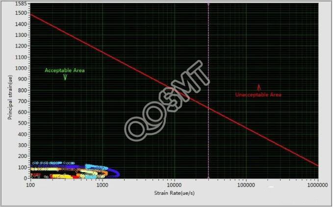
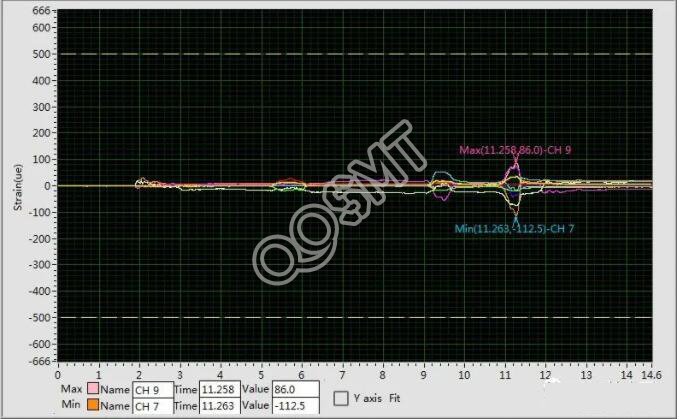
The detection and verification of sub-board stress requires a highly sensitive strain sensor (Strain Gage Sensor) and a detector (Strain Measurement Equipment). The probe of the sensor must be firmly welded or adhered to the position of the device to be measured. The fixed position must be close to the cutting edge or the device to be measured, see Figure 30C. When it comes to stress sensors, the shape is somewhat similar to a Reflow Profile thermocouple. Since the stress during the splitting is measured, the data can only be captured once during the splitting and cutting, and each sensor can only be measured once, so the cost of measurement is very high. For this reason, preparations must be done every time a measurement is performed. The measurement point must be considered to ensure that the probe is effectively fixed, and the parameters of the measuring instrument must be adjusted to the best standby (Standby) state. It should be noted that the data measured occasionally or once can usually only be used as a reference. If it is used as a basis for improvement, it needs to be measured repeatedly. If an effective test report is to be made, it will cost a lot of money. Experience has shown that the splitting method and cutting process of different plates are different, and the waveform diagrams of the stress display are often very different.
The components and solder joints of the high-density assembly board are very fragile. If the split stress is not properly controlled, it will cause hidden damage to the product. This potential failure effect will undoubtedly reduce the reliability of the product and the trust of customers. Therefore, the detection and management of the sub-board stress should become an indispensable part of the production process.
4 summary
High-density assembly boards are not only close to the limit of the distance between the components and the connecting bridges of the sub-boards, but also the circuits, components and solder joints in the board are very fragile. At the same time, the material hardness and toughness of the assembly boards are higher than that of the general substrates. The deformation stress and vibration shock wave, if not controlled or improperly controlled, can damage them. Especially the ultra-thin film highly integrated devices on the product, when imbalanced external force is applied, internal stress will be generated inside, and the internal stress will destroy the film if the internal stress exceeds the fracture critical value of the film, causing the device and module board to fail. For this reason, the interconnection design of the high-density assembly board is very particular, and its splitting process and equipment also need to fully consider the characteristics of the product. The control of the splitting stress is an indispensable and important part of the manufacturing process. .
This article introduces several common splitting techniques and equipment, focusing on the cutting-edge splitting and guillotine cutting, steel die stamping, milling cutter splitting machine, and advanced splitting technology for UV laser cutting. When evaluating the selection of sub-board equipment and technology, it is necessary to examine the size and precision of the product. It is not necessary to choose the best but the right one. It is economical, practical, efficient and safe. At the same time, this article also focuses on the panel design and cutting process of the most widely used V-Cut slot, as well as the splitting problems faced by the electric knife cutting after the conventional V-slot has evolved into different shapes. The deformed V-groove also has its unique application value on the rigid thin plate assembled with high density. By adopting the double-circular knife hand-push type cutting board splitting machine, the problem of the difficult board splitting can be better solved.
For the splitting process of high-density assembled boards, it is necessary to detect the stress and vibration wave of the splitting board after the grinding of the new product or the cutting knife of the splitting machine; to ensure that the measured data is convincing, multiple measurements may be required. A good board splitting effect should be that the milling cutter type splitting machine strives to minimize the deformation stress and vibration wave during the cutting process, so as to avoid the internal circuits, electronic devices and solder joints from stress hazards; after the splitting, the product has high accuracy, stable size and repeatability Good performance, to ensure that the cut surface is neat and smooth, etc.