SMT PCB visual inspection specifications---lines and holes
Jan 24, 2024
Foreword: As a main component of SMT, the importance of the PCB board is undoubted, so the incoming material inspection of the PCB board is also very important. The quality of the PCB board is crucial to the entire SMT assembly, so we will work with you in the near future. Discuss some key items in PCB inspection. This issue discusses the inspection specifications for lines and holes!
1. PCB circuit (Conductors) inspection specifications
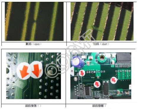
1. Open circuit, short circuit, line damage, line peeling, line deformation, etc. that affect the function are regarded as serious shortcomings (as shown in the figure below)
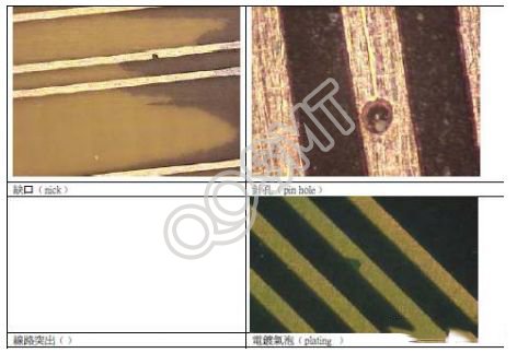
2. Gaps, pinholes, and line protrusions shall not exceed the original design line width. They are considered major shortcomings. However, common gaps and pinholes are classified as serious shortcomings.
3. Line width tolerance (inner and outer layers): The average line width of the upper and lower widths of the slice line width ≦ 5 mil: ± 20% 5 mil <line width ≦ 7 mil: ± 1 mil line width > 7 mil : ± 15% Legend: The original design line width is 5 mil, then the completed line width must be within the range of 4~6 mil, the maximum line protruding width shall not be greater than 1 mil, and the maximum line gap width shall not be greater than 1 mil, as shown in the following figure:
4. Plating bubbles generated by electroplating are regarded as major shortcomings, and if comprehensive, they are classified as serious shortcomings.
5. Circuits that are cut, worn, or scratched to expose copper are considered major defects.
6. Poor appearance caused by rough wiring is regarded as a minor shortcoming, while comprehensive shortcomings are classified as serious shortcomings.
7. No residual copper is allowed between the two lines.
8. The circuit must not cause poor appearance of the copper surface due to oxidation or contamination by chemicals or foreign matter.
9. The dents or indentations on the lines or conductors should not exceed 1/4 of the copper thickness, and the size should not exceed 20 mil. If it is comprehensive, it will be classified as a serious defect.
10. All via hole PAD and circuit connecting parts must be made by adding teardrops according to the design specifications.
2. PCB hole ﹙hole﹚: Inspection specifications
Relative position tolerance of finished holes: The relative position tolerance between any two holes in the board is ± 3 mil.
1. Tooling hole part (at least three): tooling hole diameter (position pin): 3.55+0.075/-0mm or 2.18 mm +/- 0.05 mm).
2. Non-Tooling hole part:
Via hole (including buried hole) (Hole Size≦16 mil): +2/- 4 mil.
Part hole (Hole Size >16 mil): The finished hole diameter tolerance of OSP/Immersion Gold/Immersion Silver board is +/- 2 mil, and the HASL/Lead HASL board is +/- 3 mil.
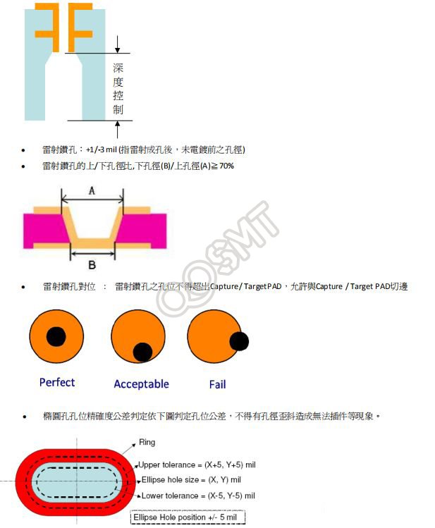
Oval hole: ±5 mil.
NPTH (including back drill) Hole Size < 5 mm: ± 2 mil. Hole Size ≥ 5 mm: ± 5 mil. Oval hole: ±5 mil.
Depth Control Hole or Depth Control Zone Depth Control Tolerance: ± 5 mil.
Engineering System
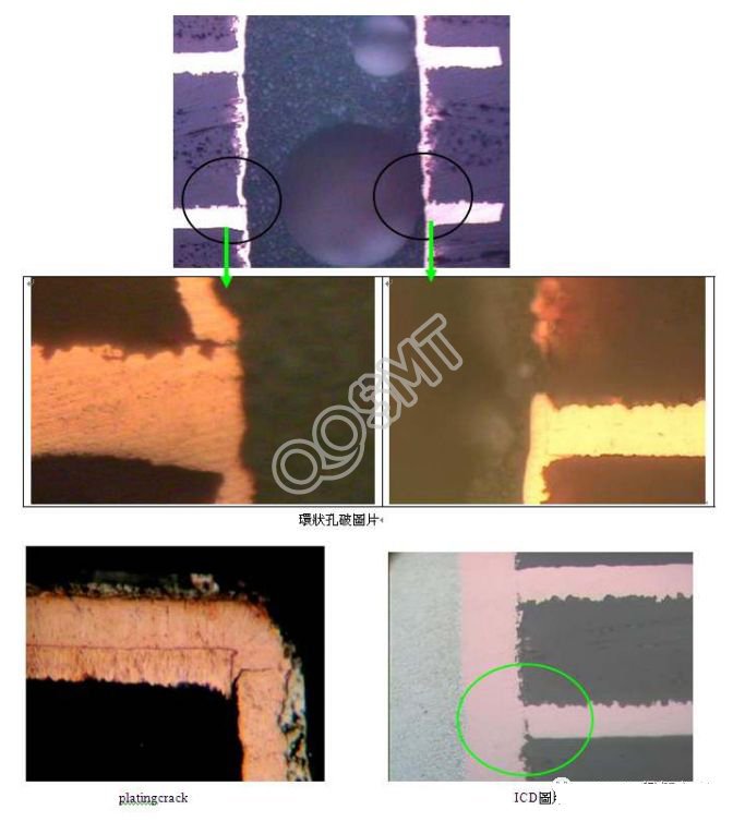
3. PTH holes are not allowed to have broken holes (including broken annular holes), plating cracks, and ICD (inter connection defects), which are regarded as serious defects, such as affecting the electrical properties of the product or Reliability will not be accepted. As shown in the slice diagram below:
4. Hole wall roughness: ≦ 1 mil.
5. If there are no special regulations, the copper thickness at the thinnest position in the hole wall of the smallest via hole must be at least greater than 0.7 mil at a single point, and the average of the six points above, middle, and below the left and right hole walls must be greater than 0.8 mil. Traditional PCB: The minimum surface copper thickness must be greater than 1.3 mil; if there is impedance control, it must also comply with its specifications. HDI PCB: The minimum surface copper thickness must be greater than 1.0 mil; if there is impedance control, it must also comply with its specifications. The actual size is subject to Micro-section.
Tin spraying on the hole wall: (1) No copper should be exposed. (2) The principle is to be able to tin.
Foreign matter in the hole: such as ink, tin plugs, green paint, plating bumps or impurities that affect the soldering resistance of the plug-in are all considered as major defects.
Laser drilling: The copper thickness at the thinnest position in the Laser drilling hole wall should be at least greater than 0.4 mil at a single point, and the average value must be greater than 0.5 mil.
Press Fit component holes: There are holes marked Press Fit on the Gerber. The single point thickness at the thinnest position must be at least greater than 1 mil.
Buried via: In the smallest via hole wall, the copper thickness at the thinnest position must be at least greater than 0.6 mil at a single point, and the average value of the upper, middle, and lower points on the left and right hole walls must be greater than 0.7 mil.
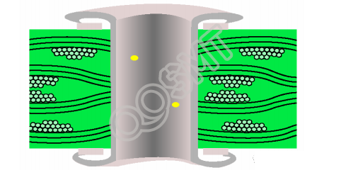
6. Hole wall plating holes (plating voids): There are no more than 2 (including 2) holes on any hole wall, and the number of holes in the entire board does not exceed 5%, and the size of any hole is Must not exceed 5% of hole length. (As shown in the picture below, the yellow part is a hole in the plating layer of the hole wall)
7. Pink ring: This phenomenon is not allowed.
8. The number of holes in the plate must be made according to the original draft, and there must be no excess or lack of holes.
9. The hole wall and the tin pad must have good adhesion and cannot be lifted, deformed or fallen off.
10. There should be no burrs, white circles (not exceeding 1.5mm) and protruding fibers around the non-plated through hole (N-PTH).
11. Rough inside the hole, tin knots, tin wire and PTH dipped in gold are not allowed. 3.2.12 There should be no tin rings or other metal objects in the openings or inside the holes of non-plated through holes (N-PTH) without tin pads.