SMT reflow soldering temperature profile (Reflow Profile) explanation and precautions
Jan 24, 2024

Preface
The reason why the electronics industry is able to flourish is that the invention and advancement of Surface Mount Technology (SMT) has made a great contribution. Reflow is one of the most important technologies in surface mount soldering technology. Here we will try to explain some of the reflow technology and temperature setting issues.
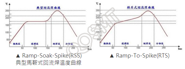
The reflow temperature profile of circuit board assembly includes four major areas: preheat (pre-heat), heat absorption (Soak), reflow (Reflow) and cooling (Cooling).
Pre-heat zone
The preheating zone usually refers to the area where the temperature rises from normal temperature to about 150°C. In this area, the temperature rises slowly (also called a primary temperature rise) so that some solvents and water vapor in the solder paste can evaporate in time, and electronic components (Especially BGA, IO connector parts) slowly heat up to prepare for the high temperature later. However, the parts on the surface of the PCB are of different sizes, and the area of the soldering pad/pad connecting copper foil is also different, and its heat absorption degree is also different. In order to avoid uneven temperature inside and outside the parts or between different parts, which may lead to deformation of the parts, Therefore, the temperature rise rate in the preheating zone is usually controlled between 1.5°C and 3°C/sec. Another purpose of uniform heating in the preheating zone is to allow the solvent in the solder paste to evaporate moderately slowly and activate the flux, because the activation temperature of most fluxes falls around 150°C.
Rapid heating helps quickly reach the temperature at which the flux softens, so the flux can quickly spread and cover the largest area of the solder joint. It allows some of the activator to be incorporated into the liquid of the actual alloy. However, if the temperature rises too fast, due to the effect of thermal stress, it may cause micro cracks in the ceramic capacitor, uneven heating of the PCB causing deformation (warpage), voids or damage to the IC chip, and the solvent in the solder paste will evaporate. Too fast will also lead to the danger of solder paste collapse.
A slower temperature climb allows more solvent to evaporate or gas to escape. It also allows the flux to be closer to the solder joint, reducing the possibility of diffusion and collapse. However, heating up too slowly can also lead to excessive oxidation and reduce the activity of the flux.
The preheating zone of the furnace generally accounts for 1/4~1/3 of the length of the heating channel, and its residence time is calculated as follows: Assume that the ambient temperature is 25°C, and if the temperature rise slope is calculated as 3°C/sec, then [(150-25) /3] is 42sec. If the temperature rise slope is calculated as 1.5°C/sec, [(150-25)/1.5] is 85sec. Usually, the time is adjusted according to the degree of difference in component size to control the temperature rise slope below 2°C/sec.
In addition, there are several undesirable phenomena related to the temperature rise in the preheating zone, which are explained one by one below:
1. Collapse:
This mainly occurs in the paste stage before the solder paste melts. The viscosity of the solder paste will decrease as the temperature rises. This is because the rise in temperature causes the molecules in the material to vibrate more violently due to heat; in addition, the temperature A rapid rise will prevent the solvent from having time to evaporate properly, causing the viscosity to drop more rapidly. To be precise, rising temperature will volatilize the solvent and increase the viscosity, but the amount of solvent volatilization is proportional to both time and temperature. That is to say, given a certain temperature rise, the longer the time, the greater the amount of solvent volatilization. Therefore, the viscosity of solder paste that heats up slowly will be higher than that of solder paste that heats up quickly, and the solder paste will be less likely to collapse.
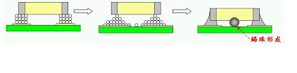
2. Tin beads:
The rapidly evaporating gas will carry the solder paste out together, forming separated solder paste blocks under the parts with small gaps. During reflow, the separated solder paste blocks will melt and pop out from under the parts to form solder beads. .
3. Solder ball:
When the temperature rises too fast, the solvent gas will quickly evaporate from the tin medium and cause splashing of solder paste. Slowing down the heating rate can effectively control the generation of solder balls. However, heating up too slowly can also lead to excessive oxidation and reduce the activity of the flux.
4. Wick siphon phenomenon:
This phenomenon is that after the solder wets the pin, the solder climbs up from the solder joint area along the pin, causing the solder joint to have insufficient solder or empty soldering. The possible reason is that during the melting stage of the solder paste, the temperature of the component pins is higher than the temperature of the PCB pads. It can be improved by increasing the temperature at the bottom of the PCB or extending the time the solder paste stays near the melting point. It is best to achieve a temperature balance between the component feet and the soldering pad before the solder is wetted. Once the solder has wetted the pad, the shape of the solder is difficult to change and is no longer affected by the temperature rise rate.
5. Poor wetting:
Generally, poor wetting is caused by excessive oxidation of the tin powder during the soldering process, which can be improved by reducing the excess heat absorbed by the solder paste during preheating. The ideal reflow time should be as short as possible. If there are other factors that prevent the heating time from being shortened, it is recommended to adopt a linear temperature from room temperature to the melting point of the solder paste, so as to reduce the possibility of oxidation of the tin powder during reflow.
6. Welding or "Head-In-Pillow":
The main reason for weak soldering may be caused by the siphon phenomenon of the lamp core or non-wetting. The phenomenon of lamp core siphon can be solved by referring to the solution of lamp core siphon phenomenon. If it is a problem of non-wetting, which is the pillow effect, this phenomenon is that the feet of the part have been immersed in the solder, but no real mutual metal or wetting has been formed. This problem can usually be improved by reducing oxidation. You can refer to Wetting Bad solution.
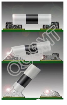
7. Tombstone effect and skew:
This is caused by uneven wetting at both ends of the part, similar to the phenomenon of lamp core siphoning. It can be improved by extending the time that the solder paste stays near the melting point, or by reducing the heating rate so that the temperature at both ends of the part is within the range of the solder paste. Equilibrium is reached before the melting point. Another thing to pay attention to is the PCB pad design. If there is an obvious difference in size, asymmetry, or one pad has a ground but no thermal relief pad, while the other pad has no Grounding can easily cause different temperatures to appear at both ends of the soldering pad. When one soldering pad melts first, the surface tension pulls the part upright (tombstone) and tilts it.
8. Voids:
This is mainly because the solvent or water vapor in the flux oxidizes rapidly and does not escape in time before the solder solidifies.
suck Soak zone
Mainly because this area is generally translated as "infiltration zone", but after teacher Bai corrected it, the correct name should be "endothermic zone", also known as "active zone". The temperature in this almost constant temperature zone is usually maintained at In the area of 150±10°C, the ramping temperature usually falls between 150 and 190°C. At this time, the solder paste is on the eve of melting, the volatile matter in the solder paste will be further removed, the activator begins to start, and Effectively removes oxides from the welding surface. The PCB surface temperature is affected by hot air convection, allowing components of different sizes and textures to maintain a uniform temperature. The board surface temperature difference △T is close to the minimum value.
(If the parts on the PCB are simple and there are not too many complicated parts, such as BGA or large parts that are easy or difficult to absorb heat, that is to say, the temperature between the parts can be easily reached uniformly, it is recommended to use the "ramp curve". Modern technology Progress, some reflow furnaces are very efficient and can quickly even out the temperature of all parts. You can also consider the "ramp-up curve". The advantage of the "ramp-up curve" is to ensure that all solder joints are melted at the same time when the solder paste melts. , the best welding effect has been achieved.)
The temperature curve shape is close to a horizontal shape. It is also a window for evaluating the reflow furnace process. Choosing a furnace that can maintain a flat active temperature curve will improve the welding effect, especially to prevent the occurrence of tombstone defects, because it is less likely to cause failure to melt tin. With a small time difference, there will be less problems with different stresses at both ends of the part.
The constant temperature zone is usually between zones 2 and 3 of the furnace, and the time is maintained for about 60 to 120 seconds. If the time is too long, it will cause excessive volatilization of rosin and cause excessive oxidation of the solder paste, which will lose its activity and protective functions during reflow soldering. As a result, problems such as weak soldering, blackened solder joint residues, and dull solder joints may occur after welding.
If the temperature in this area rises too fast, the rosin (flux) in the solder paste will expand and volatilize rapidly. Under normal circumstances, the rosin should slowly escape from the gaps between the solder pastes. When the rosin evaporates too quickly, , quality problems such as pores, blown tin, and tin beads will occur.
Reflow zone
The reflow zone is the area with the highest reflow temperature in the entire reflow section, usually also called "liquid holding time (TAL, time above liquids)". At this time, the tin in the solder will react with the copper or nickel on the pad to form an intermetallic compound Cu5sn6 or Ni3Sn4. Taking the surface treatment of OSP (organic protective film) as an example, when the solder paste melts, it will quickly wet the copper layer, and tin atoms and copper atoms will penetrate each other at their interfaces. The initial structure of the Sn-Cu alloy is a good Cu6Sn5 medium. Metal Compound (IMC), is a critical stage within the reflow oven because the temperature gradient across the assembly must be minimized. The thickness of IMC is acceptable between 1-5μm, but it is not good if IMC is too thick. It is generally recommended to control it at 1-3μm as the best. TAL must remain within the parameters specified by the solder paste manufacturer. The peak temperature of the product is also reached at this stage (the assembly reaches the highest temperature in the furnace). If the time is too long, bad IMC of Cu3Sn will continue to be generated. Boards with ENIG surface treatment will initially generate IMC of Ni3Sn4, but only a very small amount of Cu6Sn5 compounds will be generated.
Care must be taken that the temperature does not exceed the maximum temperature and heating rate capabilities of any temperature sensitive component on the PCB board. For example, a typical lead-free tantalum capacitor has a maximum temperature of 260°C that can only last for a maximum of 10 seconds. Ideally, all solder joints on the assembly should reach the same peak temperature at the same time and at the same rate to ensure that all parts experience the same environment in the furnace.
The peak temperature of reflow usually depends on the melting point temperature of the solder and the temperature that the assembled parts can withstand. The general peak temperature should be about 25~30°C higher than the normal melting point temperature of the solder paste to successfully complete the soldering operation. If the temperature is lower than this, it is very likely to cause the shortcomings of cold welding and poor wetting.
Cooling zone
e)
After the reflow zone, the product cools and solidifies the solder joints, which will prepare it for subsequent assembly processes. Controlling the cooling rate is also critical. Cooling too quickly may damage the assembly, cooling too slowly will increase TAL and may result in fragile solder joints.
It is generally believed that the cooling zone should be cooled down quickly to allow the solder to solidify. Rapid cooling can also obtain a finer fused crystal structure, improve the strength of the solder joint, make the solder joint bright, and have a continuous and meniscus-shaped surface. However, the disadvantage is that it is easier to generate holes because some gases have no time to escape.
On the contrary, slow cooling above the melting point will easily lead to the production of excessive intermetallic compounds (IMC) and larger fused crystal particles, reducing the fatigue strength. Using a relatively fast cooling rate can effectively deter the formation of intermetallic compounds.
When accelerating the cooling rate, attention must be paid to the impact resistance of the part. The maximum cooling rate allowed by a general capacitor is about 4°C/sec. Too fast a cooling rate is likely to cause stress effects and cause cracks. It may also cause peeling of the solder pad from the PCB or the solder pad from the solder joint. This is due to the different thermal expansion coefficients and shrinkage rates of the parts, solder, and solder joints. The generally recommended cooling rate is between 2~5°C/s.