SMT common process defects solutions
Oct 15, 2021


Nowadays, it is more and more convenient for engineers to make SMT patches. However, as an engineer, do you really understand the various processes in SMT? This article sorts out the "Five Major SMT Common Process Defects", to help you fill in the pit, get it quickly~!
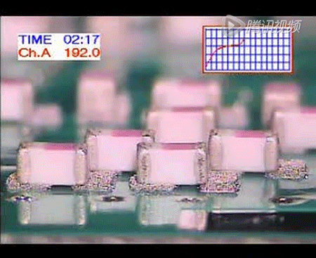
Defect one: the phenomenon of "building a stele"
(That is, the chip components are "uprighted")
The main cause of the tombstone phenomenon is the imbalance of the wetting force at the two ends of the component, which causes the torque at both ends of the component to be imbalanced, resulting in "tombstone".
Dynamic picture of reflow soldering "tombstone" phenomenon
What will cause the unbalanced wetting force at both ends of the component during reflow soldering, leading to "tombstone"? :Factor A: Unreasonable pad design and layout↓
① One of the pads on both sides of the component is connected to the ground or the area of one side of the pad is too large, and the heat capacity at both ends of the pad is uneven;
②The temperature difference across the PCB surface is too large to cause uneven heat absorption on both sides of the component pad;
③The temperature unevenness will appear at both ends of the small chip component pads around the large devices QFP, BGA, and radiator.
★Solution: Engineers adjust the pad design and layout
Factor B: There are problems with solder paste and solder paste printing↓
①The activity of the solder paste is not high or the solderability of the component is poor. After the solder paste is melted, the surface tension is different, which will cause the pad wetting force to be unbalanced.
②The amount of solder paste printed on the two pads is uneven, the printing is too thick, and the excess solder paste overflows after the component is pressed down; ②The mounting pressure is too large, and the pressing down causes the solder paste to collapse onto the ink; ③The shape of the pad opening is not good , No anti-tin bead treatment; ④The activity of the solder paste is not good, it dries too fast, or there are too many small tin powders; ⑤The printing offset makes part of the solder paste stick to the PCB; ⑥The squeegee speed is too fast, Causes poor collapse and solder balls after reflow...
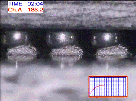
Defect three: bridging
Bridging is also one of the common defects in SMT production. It will cause short circuits between components, which must be repaired in case of bridging.
BGA bridge diagram
The main reasons for bridging are:
Factor A: the quality of solder paste ↓
①The metal content in the solder paste is too high, especially if the printing time is too long, the metal content is likely to increase, which leads to bridging of IC pins;
②The solder paste has low viscosity and flows out of the pad after preheating;
③The drop of the solder paste tower is poor, and it flows out of the pad after preheating;
★Solution: the factory needs to adjust the solder paste ratio or use good quality solder paste
Factor B: Printing System↓
①The printing machine has poor repeat accuracy and misalignment (inaccurate stencil alignment, inaccurate PCB alignment), causing solder paste to be printed outside the pads, especially fine-pitch QFP pads;
②The design of the size and thickness of the steel mesh window is inaccurate, and the Sn-pb alloy coating of the PCB pad design is uneven, resulting in too much solder paste;
★Solution: The printing machine needs to be adjusted by the factory to improve the coating layer of the PCB pad;
Factor C: Excessive pressure on post and release↓
The full flow of solder paste after pressure is a common reason in production. In addition, insufficient placement accuracy will cause component displacement and IC pin deformation;
Factor D: The heating rate of the reflow soldering furnace is too fast, and the solvent in the solder paste is too late to volatilize
★Solution: the factory needs to adjust the height of the Z-axis of the placement machine and the heating rate of the reflow soldering furnace
Defect four: wicking phenomenon
Wicking phenomenon, also known as suction phenomenon and core pulling phenomenon, is one of the common soldering defects of SMT, which is more common in vapor reflow soldering. The solder detaches from the pad and travels along the pin to between the pin and the chip body, causing serious virtual soldering.
Cause ↓:
Usually because the thermal conductivity of the lead is too large, the temperature rises rapidly, so that the solder preferentially wets the lead, the wetting force between the solder and the lead is much greater than the wetting force between the solder and the pad, and the upturn of the lead is more Will aggravate the occurrence of wicking.
★Solution: The factory needs to fully preheat the SMA (surface mount component) and then solder in the furnace. The solderability of the PCB pads should be carefully tested and ensured. The coplanarity of the components cannot be ignored. Devices with poor performance should not be used in production.
Note: In infrared reflow soldering, the organic flux in the PCB substrate and solder is a good infrared absorbing medium, but the pins can partially reflect infrared, so the solder is preferentially melted by comparison, and the wetting power of the solder and the pad It will be greater than the wetting force between the solder and the pin, so the solder will not rise along the pin, so the probability of wicking phenomenon is much smaller.
Defect five: BGA welding is poor
BGA: Ball Grid Array (ball grid array package)
Below: Normal BGA welding
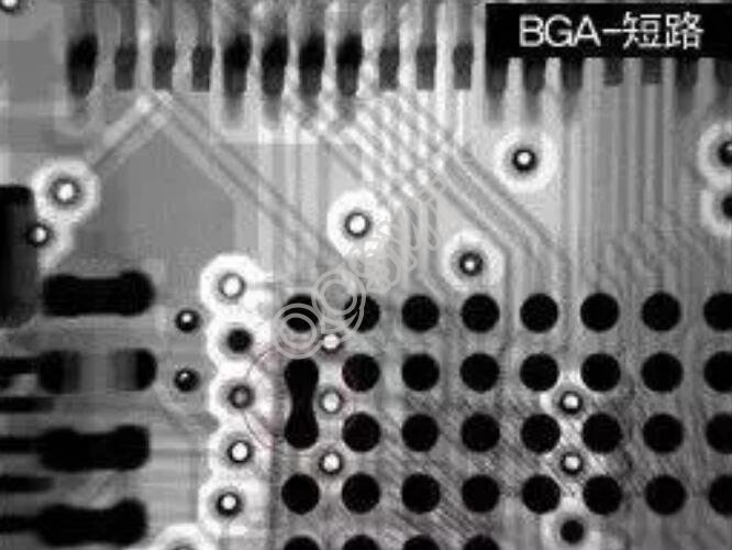
Adverse symptoms①: Lianxi↓
Connecting tin is also called a short circuit, that is, the solder ball and the solder ball are short-circuited during the soldering process, which causes the two pads to be connected, resulting in a short circuit.
★Solution: the factory adjusts the temperature curve, reduces the reflow air pressure, and improves the printing quality
Schematic diagram of connecting tin: the part in the red circle is connecting tin
Adverse symptoms ②: false welding ↓
False soldering is also called "Head-in-Pillow (HIP)". There are many reasons for false soldering (oxidation of solder balls or PAD, insufficient temperature in the furnace, PCB deformation, poor solder paste activity, etc.). BGA false welding is characterized by "difficult to find" and "difficult to identify".
Schematic diagram of BGA false welding
Side view of BGA "pillow effect" (source network)
Adverse symptoms ③: cold welding↓
Cold soldering is not exactly the same as false soldering. Cold soldering is caused by the abnormal reflow temperature causing the solder paste to not melt completely. It may be caused by the temperature not reaching the melting point of the solder paste or insufficient reflow time in the reflow zone.
★Solution: the factory adjusts the temperature curve to reduce vibration during the cooling process
Schematic diagram of BGA cold welding
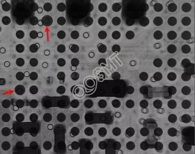
Adverse symptoms④: bubbles↓
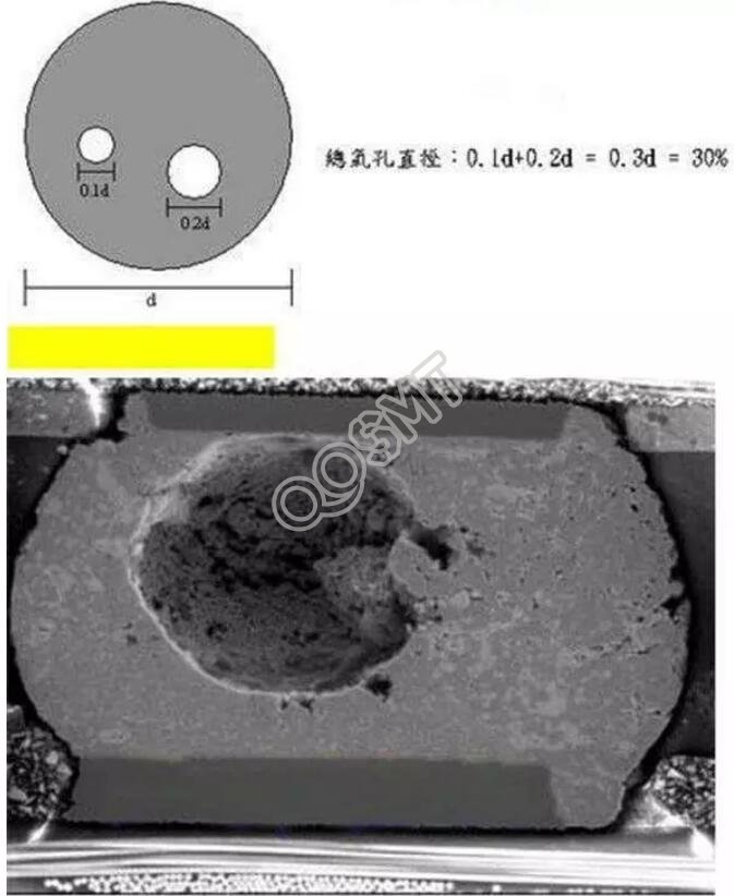
Bubbles (or pores) are not an absolute bad phenomenon, but if the bubbles are too large, it is easy to cause quality problems, and the acceptance of bubbles has IPC standards. The air bubbles are mainly caused by the air in the blind hole not being discharged in time during the welding process.
★Solution: require the factory to use X-Ray to check whether there are pores in the raw material and adjust the temperature curve
BGA bubble diagram
Generally speaking, the bubble size cannot exceed 20% of the sphere
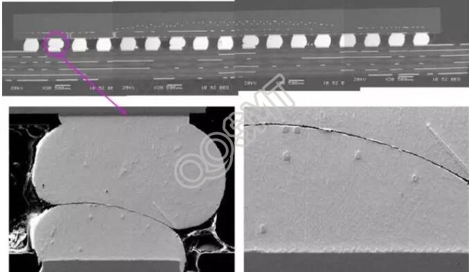
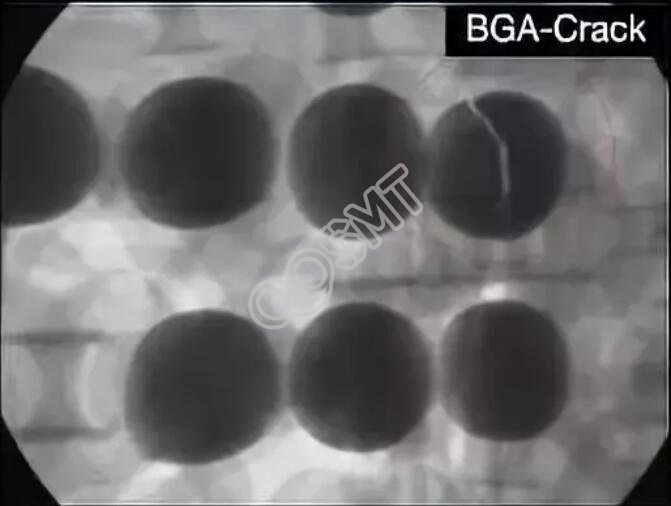
Adverse symptoms ⑤: solder ball cracking↓
Adverse symptoms ⑥: Dirty ↓
If the pad is dirty or has residual foreign matter, it may be due to poor environmental protection during the production process that there is foreign matter on the pad or the pad is dirty, which may lead to poor soldering.
In addition to the above points: ① crystal cracks (the surface of the solder joints are glass cracks); ② offset (the BGA solder joints are misaligned with the PCB pads); ③ tin splashing (there are tiny tin balls on the surface of the PCB close to or introduced) Between two solder joints) and so on.