* We will reply you within 24 hours.


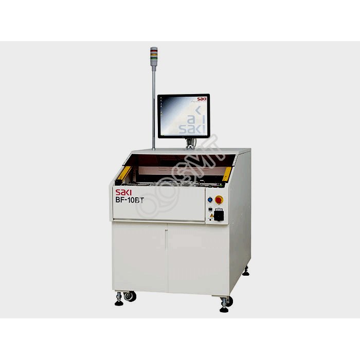
SAKI 2D AOI BF-10BT AOI Inspection Equipment
Board Size 50 x 50 - 250 x 330mm
Board Thickness 0.6mm - 3.2mm
Dimensions 850× 1405× 1130
Board Thickness 0.6mm - 3.2mm
Dimensions 850× 1405× 1130
Brand Name:
SAKI
Model:
BF-10BT
Condition:
New / Used
Payment Methods
The ultimate machine for double-sided PCB inspection, the BF-10BT's robust and highly repeatable system is built for 24/7 continuous operation. The system inspects both sides of the PCB in one process with 10μm resolution. It inspects 01005 in. (0402mm) components and detects solder balls down to 150μm with high speed and superior data handling capabilities. It's perfect for final inspection, through-hole inspection after wave or selective soldering, or manual inspection.
The offline inspection machine series can directly contribute to improve line productivity with shorter tact time.
By employing telecentric lens optical system, BF-10BT provides accurate and stable inspection results. Off-line Simultaneous Double-SidedAutomated Optical Inspection System
BF-10BT is the automated optical inspection system which inspectsboth sides of double-sided PCBs at once. Due to this the system achieves the same inspection speed as single side inspectionsystems. It is equipped with two cameras for scanning per eachside of a PCB using Saki's unique alternate scanning technology. Ithas 40 mm clearance on both sides; therefore it is suitable for thefinal inspection process after all component assembly.
Machine Overview
The BF-10BT has been developed for the end of line inspection, it performs a simultaneous Automatic Optical Inspection of both sides of the PCB. It fully inspects both SMD and hand placed parts including PTH.BF-10BT can detect overlooked defects from earlier processes and improve the quality of your products.
Simultaneously Inspects Both Sides of PCBs
BF-10BT is the automated optical inspection system which inspects both sides of double-sided PCBs at once. Due to this the system achieves the same inspection speed as single side inspection systems. It is equipped with two cameras for scanning per each side of a PCB using Saki's unique alternate scanning technology. It has 40 mm clearance on both sides; therefore it is suitable for the final inspection process after all component assembly.
Reducing Inspection Process
In a double-sided PCB mounting process, defects might occur on Side A during the mounting process of Side B. In order to find such defects, two inspection machines and a PCB flipper are usually needed for the final inspection process. Installation of BF-10BT, integrates all of these systems into one.
Suitable for Final Inspection
Process BF-10BT is capable of inspecting both sides simultaneously at high speed. It is a suitable solution for the final process. However it is also be a solution for acceptance inspection post SMD before back end assembly process.
Coaxial Overhead Light
Soldering condition is inspected by illuminant irradiation of coaxial overhead lighting. With the use of coaxial lighting shadows are not generated and, the inspection is not affected by the shadow of neighboring tall components. Therefore, the same library is fully usable at any location of the board
Real-time Defection Management and Analysis
With the real-time SPC display function, BF-10BT provides the real- time production management enabling efficient productivity and quality. It can be networked with an extensive range of optional systems (BF- Editor/BF-RP1/BF-View) to provide off line programming, paperless rework and inspection history.
High Resolution Imaging SystemWith 10 μ m resolution, BF-10BT provides accurate and stable inspection of 0402 mm (01005 in.) chips. The newly developed color capturing system takes only 8 seconds to scan M-size board (250 x 330 mm, 10 x 13 in.).
Advantage of Line Scan Visual Inspection
Extra components on a PCB can be detected by setting up only one inspection window for the whole board. This advantage is offered thanks to our line image acquisition technology means that any damage such as scratches, solder balls or contamination on side A resulting from side B assemble can be found.
Improved Operability
In addition to "Start Button", BF-10BT is equipped with "OK /NG Button" so that the operator doesn't have to use keyboard or mouse during its automatic operation
| Model | SAKI 2D AOI BF-10BT |
| Resolution | 10μm |
| Board Size | 50 x 50mm - 250 x 330mm |
| Board Thickness | 0.6mm - 3.2mm |
| Board Warp | +/-1mm |
| PCB Clearance | Top: 40mm, 1.57in. Bottom: 40mm(*1) |
| Rotated Component Support | Available for 0 - 359°rotation (unit of 1°) |
| Inspection Categories | Presence/Absence, Misalignment, Tombstone, Reverse, Polarity, Bridge, Foreign material, Absence of solder, Insufficient solder, Lifted lead, Lifted Chip, and Fillet defect. Each defect name can be changed freely by system function. |
| Tact Time | Approx. 14 sec.(*2) (*3) (250×330mm) |
| Image Scanning Time | Approx. 8 sec.(*2) (250×330mm) |
| Camera (Image Processing) | Line color CCD camera |
| Lighting | LED lighting system |
| Transfer Conveyor Method | Flat belt transfer |
| Transfer Conveyor Height | 900+/-20mm, 36+/-0.8in |
| Transfer Conveyor Width Adjustment | Manual |
| Operating System | Windows XP English Version |
| Optional System | BF-Editor / BF-RP1 / BF-Monitor / BF-View |
| Optional | 2D Barcode Recognition, Journal Printer, BlackLight (Conformal Coating Inspection) (*4) |
| Electric Power Requirement | Single Phase ~100-120V/200 to 240V+/-10%, 50/60Hz, 800VA |
| Air Requirement | 0.5MPa, 5L/min (ANR), 73PSI, 0.18CFM |
| Usage Environment |
15°C(59F) - 30°C(86F) / 15 - 80% RH (Non-condensing) |
| Noise Level | 58.3dB |
| Dimensions W x D x H | 850(W) × 1405(D) × 1130(H)mm |
| Weight | Approx. 420kg |
|
(*1) e.g. when a PCB’s thickness and warp are 1 mm, the top clearance is 38 mm and the bottom clearance is 40 mm from the PCB surface. (*2) If a PCB size is smaller than 250x330mm, image scanning time will be shorter than these values. (*3) Including image scanning time. (*4) When choosing this optional, PCB Clearance is Top : 30 mm, Bottom : 30 mm. |
|
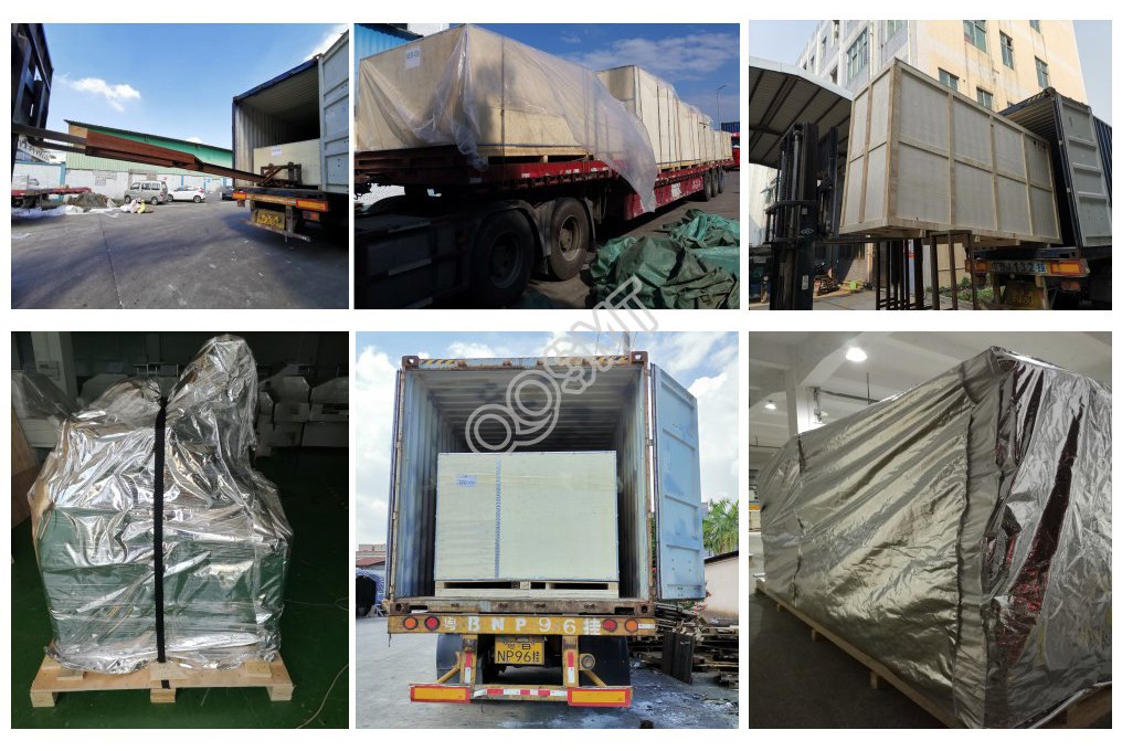
Ensure your ordered products are always safely packaged fast delivery to your hands

